a few examples of my work
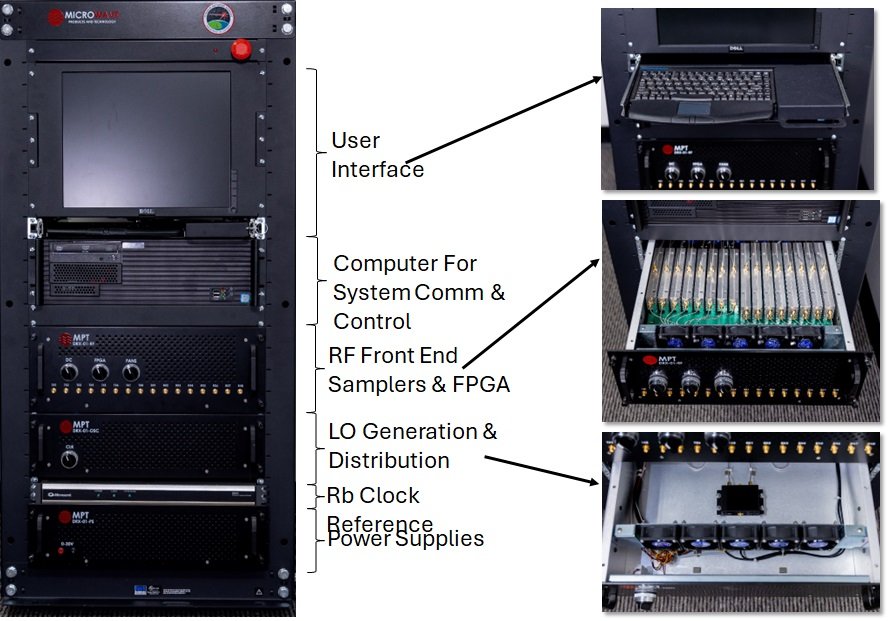
System Design Example: DREX Developed For X-Band Phased Array Radar
I figured I should show an example of a system I developed. Well, it was really a complex subsystem, but with nearly all complex subsystems, we considered it a system–Yes, I know it is not technically correct. However, for anyone who has worked on a major platform development this is not unusual.
For instance, when I was doing R&D on phased array radars for airborne applications, we considered the radar to be a system. However, to the air frame guys, the radar was just another component that went into the airplane. But enough of that.
The Digital Receiver/Exciter (DREX) had eight channels of transmit, eight channels of receive, low noise figure, wide dynamic range, and supported very wide instantaneous bandwidth. We were sampling at approximately 5GS/s on receive and approximately 10GS/s on transmit. Transmit power was approximately 10dBm. The outputs were fed to high power amplifiers in T/R modules. We had very complex down converters with state of the art functional features. The details on the performance can’t be shared here.
A Favorite Microwave Circuit Of Mine Is A Balun
I have designed many different types of RF and microwave circuits during my career including MMICs, mixers, amplifiers, filters, couplers, diplexers, high power amplifiers, and so many others. However, one of my top 10 favorite circuits is a balun.
I am not sure why I like designing baluns so much, but I think there may be two contributing factors. First, I learned about baluns from Dr. Stephen Maas when I was a graduate student at UCLA. He did such a great job explaining them to us, that I had the confidence as a young engineer to design them. Second, they are used in so many different types of microwave products such as antennas, mixers, and diode frequency multipliers. I think these two facts contribute to my affinity toward baluns.
Simply put, a balun converts an unbalanced transmission line such as coax to a balanced line such as a parallel line transmission line. An important characteristic is that for a true balun, the impedance from any one of the balanced outputs to ground is infinite, or at least very high. Also, the outputs are 180 degrees out of phase with each other. A more rigorous definition exists, but that’s good enough for here.
In practice, plenty of very useful baluns have been used in circuits that don’t have a large impedance from any one of the balanced outputs to ground. In fact, I’ll describe one of them next.
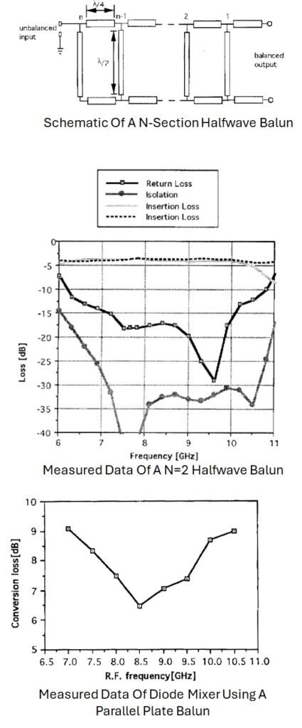
The figure to the left shows an n-section halfwave balun. It’s more accurately described as a quasi-balun since the impedance between the “balanced” outputs and ground is about 50 ohms instead of infinite or very large. Nevertheless, this circuit acts like a decent balun for diode mixers and frequency multipliers. The measured data for a n=2 balun of this type is also shown in the figure.
I’ve used a parallel plate balun to design and fabricate many different diode mixers and multipliers. The figure to the left shows the measured conversion loss of a diode mixer using a parallel plate balun. It was designed to work from 8 to 10GHz. These are just a few examples of balun circuits I have developed. Maybe I’ll post some of the antennas I have developed that use baluns.
Materials Characterization For Accurate Packaging Design
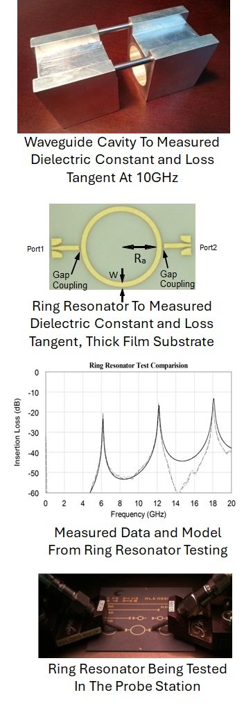
When designing packaging solutions, it is critical to have accurate materials data such as dielectric constant and loss tangent. As a result, I have used many different methods to characterize the dielectric constant and loss tangent of the materials I have used. The image to the left shows a few of the techniques I have used. I have settled on three methods that I prefer:
1. Circular cavity method as shown in the top figure to the left. It shows my split waveguide resonator test fixture. It allows me to perform non-destructive tests on dielectric substrate slides that I can later use to fabricate circuits. I can also use planar substrate material samples from suppliers. This technique is both high precision and high accuracy and it is non-destructive for planar samples like dielectric substrates.
2. The ring resonator method is shown in the figure to the left. It works well, but measurements are best performed at a probe station as shown in the lower image for very accurate data gathering. I have found it to be more accurate in determining dielectric constant than loss tangent since some assumptions must be made about the contribution of the conductor loss to the measured resonance Q.
3. Another method is the waveguide insertion method. In this method, I’ve used rectangular waveguide with material samples of various lengths prepared to slide perfectly inside the waveguide with minimal gap to the side walls and top/bottom walls. I have used this method from 10GHz to 94GHz and it works very well for both determining dielectric constant and loss tangent.
I’ve used other methods, but these are my three favorites.
R. Sturdivant, “Materials and transmission line measurements comparing HTCC and Thick Film Alumina,” From: 2014 IMAPS Ramp Conference, San Diego. (download my writeup here)
R. Sturdivant, “Millimeter-wave characterization of several substrate materials for automotive applications,” In Proceedings of Electrical Performance of Electronic Packaging,” Oct 2-4, Portland, 1995. (download the article here)
Aluminum Nitride (AlN) For High Power Amplifier Packaging RF Performance And Moisture Effects
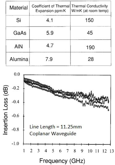
I did some research on comparing substrate materials for microwave circuits–especially for high power amplifier modules. My research focused on aluminum nitride because of its high thermal conductivity. However, very little was known about it for use in microwave electronic packaging.
At the time, there were concerns about interactions of AlN to moisture. Specifically, the effects of moisture on the microwave performance of AlN substrates. Specifically, I needed to show that AlN electrical performance parameters I was interested in do does not change when exposed to moisture.
The figures show a comparison AlN to other substrate materials. It also shows measured insertion loss of a 11.25mm long conductor backed coplanar waveguide (CBCPW) transmission line.
I was able to show that AlN does not change insertion loss in a measurable way when soaked in 10 megohm high resistivity water for 27 days and then boiled in water for 8 hours.
R. Sturdivant, “Heat dissipating transmission lines,” Applied Microwave and Wireless, Spring 1995.
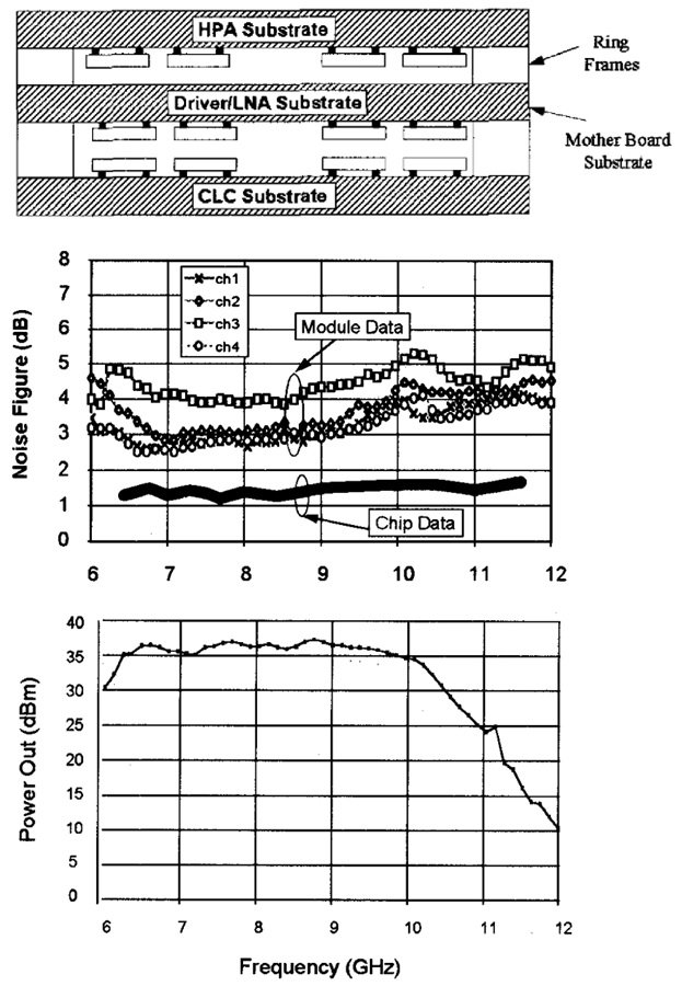
Aluminum Nitride T/R Module With Flip Chip MMICs
Years ago, I developed a high power transmit/receive (T/R) module for an airborne radar application. The technology for the module is called Tile Array. Each module had four T/R channels. I describe it in my book Transmit Receive Modules For Radar and Communication Systems (Artech House, 2018). There are several characteristics of this module that made it unique at the time:
1. Aluminum Nitride (AlN) co-fired ceramic was used for the substrates. The substrates had approximately 8 layers of internal routing. AlN was chosen for its superior thermal performance at approximately 160-190W/mK thermal conductivity.
2. The integrated circuits were flip chip GaAs MMICs and Si ICs. Flip chip GaAs MMICs were a significant innovation at the time.
3. Stacked ceramic substrates with solderless interconnects between them using compressible fuzz buttons.
4. The substrates that contained lower power dissipation circuits like low noise amplifiers (LNAs) used Low Temperature Cofired Ceramic (LTCC) since it was lower cost and had some other attractive features. LTCC at the time had a thermal conductivity of approximately 2-4 W/mK.
In short, the module I developed was a major success and the design was deployed on multiple airframes. The figures to the left show the measured noise figure of the module compared to the LNA noise figure. The output power as approximately 4W which was a respectable amount of T/R module power at the time.
R. Sturdivant, et.al., “Design and Performance of A High Density 3D Microwave Module,” In Proceedings of IEEE MTT-S Symposium.
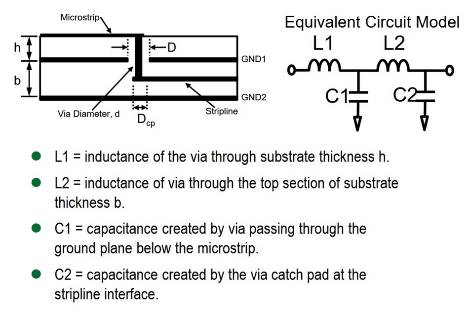
A Packaging Transition I Have Used at Least A 100 Times--The Microstrip To Stripline Transition
As frequency increases, the physical size of the features used in the routing of RF signals become large. This is especially true for complex transitions between transmission line types.
The figure to the left shows a transition from microstrip to buried stripline. I have used this transition so many times in various types of products from phased arrays to up/down converters and filter banks. It is very useful when moving signals from one part of a product to another where isolation and packaging density are a concern.
Careful design practices must be used. The figure to the left shows four circuit elements that account for the stray capacitive and inductive effects present in the transition. While it is challenging to make this type of transition function well, it is possible for it to function over very wide frequency ranges when carefully designed.
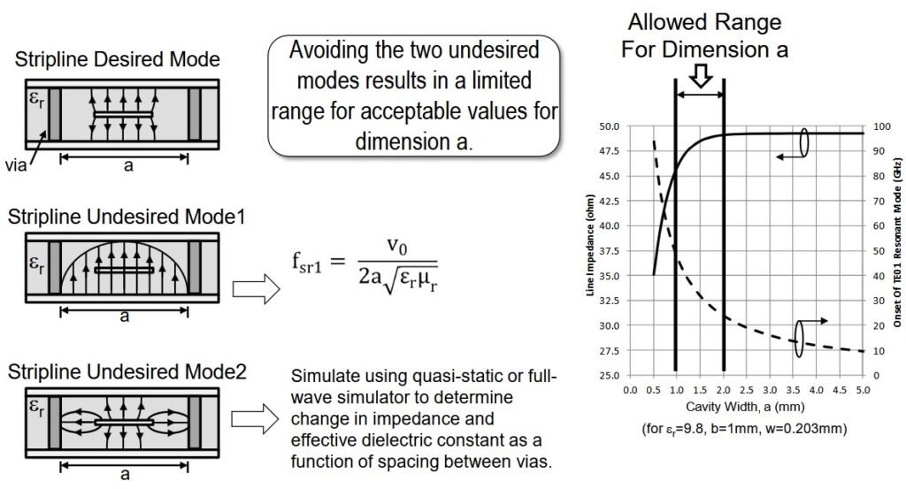
Stripline Design Guideline
In my book Microwave and Millimeter-wave Electronic Packaging (Artech House, 2014), I described some guidelines on transmission line design. One of them I mentioned is the avoidance of higher order modes in stripline designs. This is especially important for multilayer RF circuit boards that often use buried stripline.
Two undesired modes are: 1) The waveguide mode and I show the equation for calculating it’s cut off frequency. 2) The ground via coupled mode which lowers the line impedance of the transmission line due to the extra capacitance. It also increases the line loss due to edge current crowding on the stripline. BTW, there are many other undesired modes, but their cutoff frequencies will be well out of the band you design with as long as you follow my suggestions here which are described in more detail in my book.
Bottom line, if you are designing in stripline, avoid these undesired modes and follow other transmission line design guidelines I provide in my book.
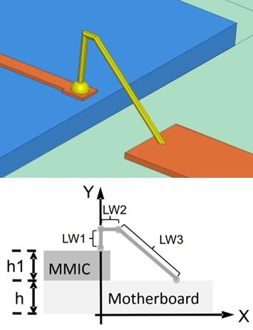
Wire Bond Modeling To 50GHz For MMIC Packaging
As part of a MMIC packaging project I was working on, I needed to have an accurate parameterized model of wire bond that was being used. The application was a wide band system operating from about 1GHz to approximately 45GHz.
I performed a series of parameterized HFSS simulations and imported those results into a microwave circuit simulator where an equivalent circuit was developed. I then performed a multidimensional optimization to match the magnitude and phase of S11 and S21 between the HFSS model and the equivalent circuit I generated. The optimization was performed over the frequency range of 1 to 50GHz. The figure below shows the model and the agreement of the model over the frequency range.
These days, there is software available that will extract the equivalent circuit. However, that software did not exist at the time. Regardless, if I had to do it again today, I would likely use the extraction tools that are available, but I woud certainly do some serious validation of the extraction.
R. Sturdivant, “Broadband electrical modeling of transitions and interconnects useful for PCB and Co-Fired Ceramic Packaging,” ISHM Packaging Conference, 2014.
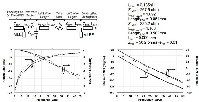
X-Band & Ku-Band Diplexer
Some years ago, I developed a low insertion loss diplexer for use in a wide band phased array system.
For this design, I used suspended substrate stripline (SSS) to form a band pass & low pass filter diplexer. I chose SSS for several reasons. First, it is low insertion loss when compared to other transmission lines like microstrip and coplanar waveguide. Second, for a filter design, it offers improve Q over the alternatives. Third, the packaging for it used a split housing design which was compatible with the rest of the system.
I designed the diplexer and used HFSS plus a few custom models I developed within the circuit simulator. For the Ku-Band band pass output, I developed a model for the capacitive overlap section and that model is documented here [1]. For the transmission lines, I used a model for line impedance and effective dielectric constant of the transmission lines based on a parametric set of HFSS simulations. These HFSS based circuit models allowed me to rapidly optimize the design in a circuit simulator and then transfer the design to HFSS for a full simulation.
I built the diplexer and measured its performance. Here are a few important performance parameters.
Crossover Frequency = 11GHz
Low Pass Insertion Loss = 0.5dB
Band Pass Insertion Loss = ~1.0dB (0.8dB to 1.2dB)
[1] R. Sturdivant, “A capacitively coupled BPF design using a suspended substrate stripline,” Microwave Journal.
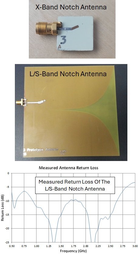
Images showing a X-Band tapered slot notch antenna, a L/S-Band tapered slot notch antenna, and the measured return loss of the L/S-Band tapered slot notch antenna.
Tapered Slot Antennas
A tapered slot antenna (TSA) is a directional antenna characterized by a gradually widening slot that efficiently guides and radiates electromagnetic waves. A variant of a tapered slot antenna is a notch antenna … well notch antenna is not a widely accepted description of it. The name was coined by Dr. Cheng Peng who has several patents on them and his patents call it a Notch antenna, so maybe that really is what it should be called. Nevertheless, Dr. Peng trained me to use that name, so I’ve stuck with it.
Known for their wide bandwidth and high gain, TSAs are widely used in radar, wireless communications, and high-resolution imaging systems. Their broadband performance makes them ideal for applications requiring reliable operation across a broad frequency range.
I have extensive experience in the design and development of tapered slot antennas, delivering solutions that operate seamlessly from 600 MHz to 35 GHz. My expertise encompasses the entire development process, from initial design and simulation to material selection and performance optimization.
The images to the left show two notch antennas, which are, as I explained above a type of TSA. If you look closely you can barely make out the tapered slot on the bottom copper of the L/S-Band antenna.
You can download some measured data of the X-Band tapered slot antenna here.
R. Sturdivant, E.K.P. Chong, “Dielectric notch radiator antennas with integrated filtering for 5G and IoT access,” In Proceedings Of 2017 IEEE Radio and Wireless Symposium (RWS), Jan 15-18, Phoenix, AZ.
Spiral Antenna
A spiral antenna is a type of frequency-independent antenna known for its wide bandwidth, circular polarization, and compact design. It is commonly used in applications such as direction finding, satellite communications, and radar systems due to its consistent performance across a broad frequency range and ability to handle multiple polarizations.
I have extensive experience in designing and developing spiral antennas, creating solutions tailored for various applications and frequency requirements.
My expertise includes optimizing performance characteristics such as impedance matching, axial ratio, and beamwidth.
I have successfully developed multiple high-performance spiral antennas, delivering reliable, innovative designs that meet complex engineering demands.
For information on the measured performance of this spiral antenna I designed, you can find it here.
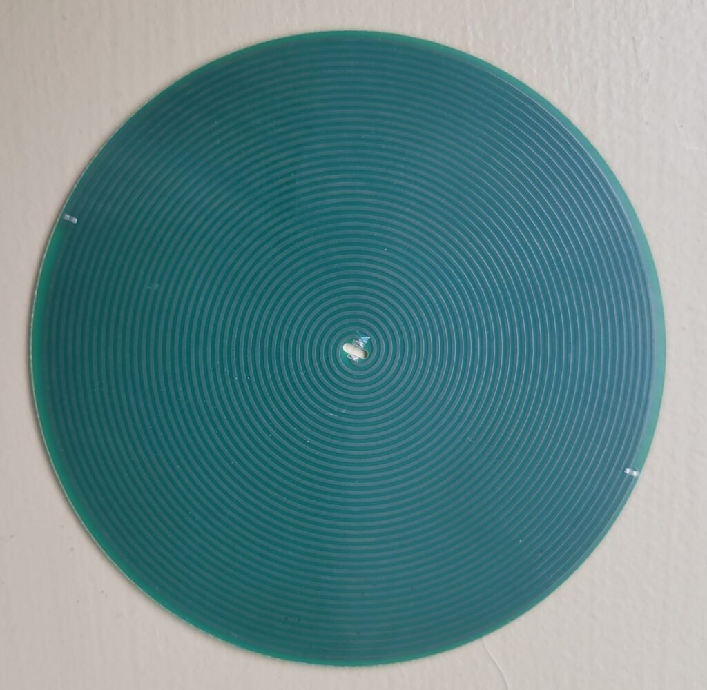
Image of a spiral antenna I designed to operate at L-Band. It was designed for right hand circular polarization and had excellent axial ratio, gain, and impedance match.
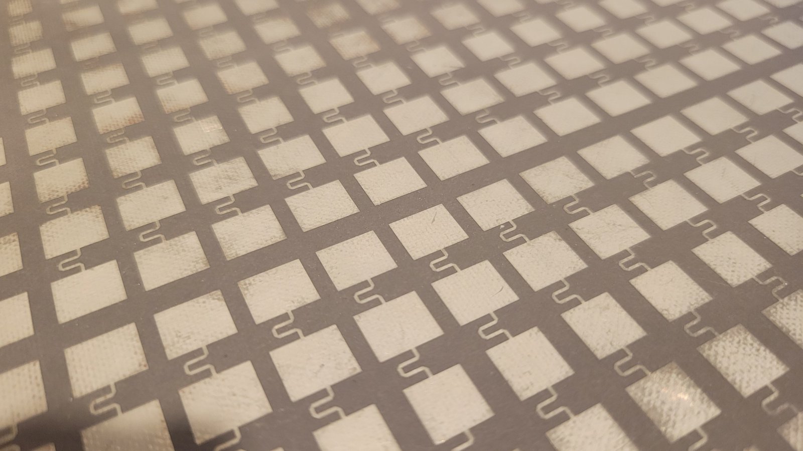
Image of a phased array using patch antenna elements.
Phased Arrays
Your phased array requirements may seem unclear or challenging for you to meet in the timeline required. My proven phased array development process will help guide you to the solution.
From concept to deployment, the process is crafted to result in innovative designs that optimize beamforming, coverage, and signal performance.
The phased array solutions are tailored to deliver precision, reliability, and efficiency, ensuring your systems excel in complex environments. With a focus on streamlined development cycles and cutting-edge technology, I address your specific challenges while delivering superior results.
Whether for defense, aerospace, or telecommunications, my expertise ensures your phased array systems achieve unparalleled performance and a competitive edge. Let’s bring your vision to life.
For more information on phased arrays, I suggest my book title Systems Engineering of Phased Arrays which is available on Amazon or from the publisher.
Or, for an example of a phased array design applied to satellite communications you can download an article I wrote here.